Lab 2: Multiplexed 7-Segment Display
Introduction
This lab introduced us to managing I/O on our FPGA by turning the single seven segment display from Lab 1 into a dual seven segment display! Instead of doubling the amount of I/O pins used to program the display, we were tasked with implementing time-multiplexing to control the two displays. This lab was important in teaching us how to properly manage clocks and ensuring we followed synchronous sequential design principles even as our hardware becomes more complex. See the E155 Lab 2 Page for a more detailed overview of the specifications and instructions for this lab.
All code written for this lab can be found on my E155 Lab 2 Repository on Github.
Setup and Circuitry
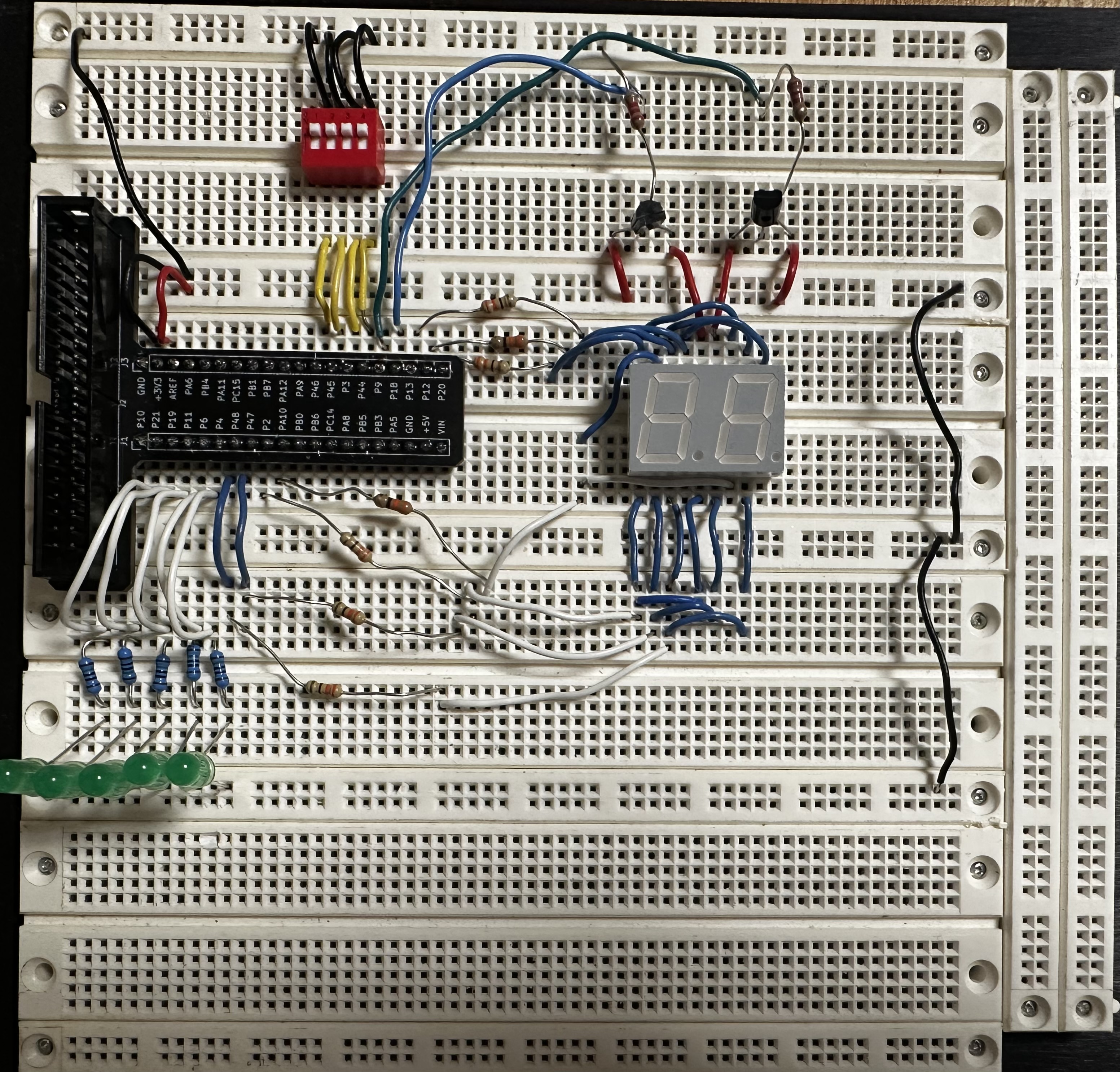 A picture of my completed circuit!
On the left is a picture of my final circuit setup, the circuit diagram for this circuit is shown at the bottom of this section. Two transistors were used to carry out
the time-multiplexing as a signal was sent to each controlling which display received power at any moment. Since the gate of the transistors were
connected to I/O on the FPGA, it was important to ensure there was not too much current being drawn from the FPGA pins. I used the following expression
to calculate resistor values. From the datasheet for the FPGA, the maximum current
draw for maintaining logic levels is 8 mA.
\[ R = (V_{cc} - V_{LED}) / I_{max} \]
\[ R = (3.3V - 0.7V) / 0.008A = 325 Ohms\]
A picture of my completed circuit!
On the left is a picture of my final circuit setup, the circuit diagram for this circuit is shown at the bottom of this section. Two transistors were used to carry out
the time-multiplexing as a signal was sent to each controlling which display received power at any moment. Since the gate of the transistors were
connected to I/O on the FPGA, it was important to ensure there was not too much current being drawn from the FPGA pins. I used the following expression
to calculate resistor values. From the datasheet for the FPGA, the maximum current
draw for maintaining logic levels is 8 mA.
\[ R = (V_{cc} - V_{LED}) / I_{max} \]
\[ R = (3.3V - 0.7V) / 0.008A = 325 Ohms\]
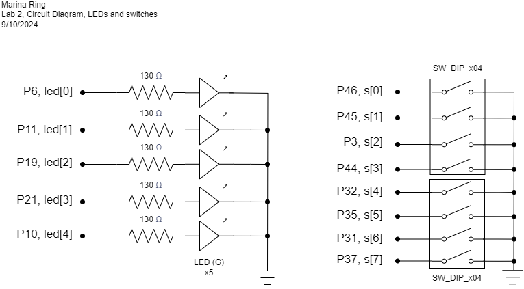
I ended up using a resistor of 1.2 kOhms just to be safe. I also made sure that the green LEDs I used to display the sum of two numbers had the appropriate current-limiting resistors.
I used Ohm's Law again, considering a 2V voltage drop across one LED.
\[ R = (V_{cc} - V_{LED})/ I \]
\[ R = 3.3V - 2V/ 0.01A = 130 Ohms \]
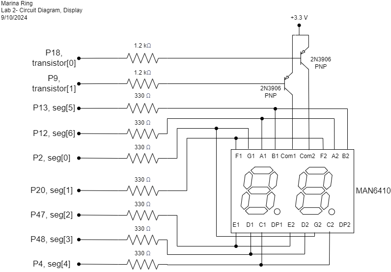
The circuit schematic below details the Upduino pins I used to power the display and LEDs. Since the MAN6410 is a common anode display, 3.3V is supplied at the
anode and each pin acts as a cathode. To turn a segment on, a pin is set to low or 0 and so current can flow down that path. To turn a segment off, the pin is
set back to high or 1. The pin assigments are displayed in the circuit diagrams below.
Software and Verification
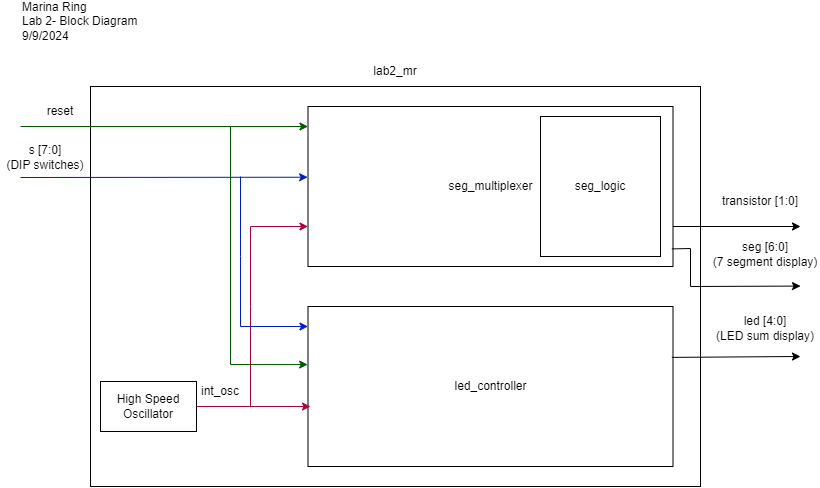 A block diagram model for this system.
On the left is a block diagram visualizing the Verilog modules that I used in this lab and their inputs, outputs, and connections. I created separate modules to control the LEDs displaying the sum
of the two digits and to control the display itself. This was done to individually isolate each system to debug them separately. In particular, the multiplexing module was more complicated to debug,
so separating it from other modules made testing other functions of this design easier.
A block diagram model for this system.
On the left is a block diagram visualizing the Verilog modules that I used in this lab and their inputs, outputs, and connections. I created separate modules to control the LEDs displaying the sum
of the two digits and to control the display itself. This was done to individually isolate each system to debug them separately. In particular, the multiplexing module was more complicated to debug,
so separating it from other modules made testing other functions of this design easier.
The FPGA outputs a 24 MHz clock, but I found this too fast for multiplexing as the propagation time through the circuit is slower than the clock switching, causing the displayed digits to "bleed" together. It is found that humans can potentially distinguish flickering up to 500 Hz, so I decided that a frequency around 1-5 kHz would be sufficient for multiplexing. I chose a 12 bit counter to produce a frequency of around 3 kHz. The digit that is powered changes once the counter overflows, or after each digit is 1. \[ f_{digits} = f_{clk}/(2*2^{N}) \] \[ f_{digits} = 24*10^{6}/2*2^{12} = ~3 kHz\]
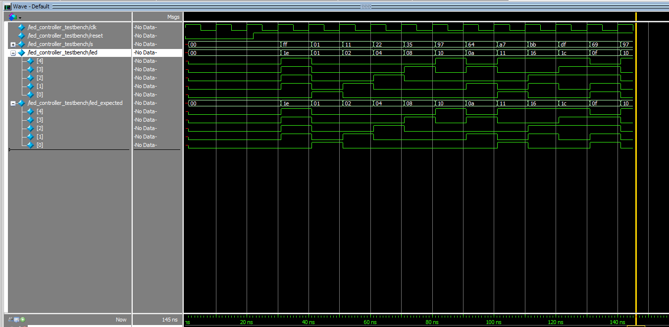
I wrote a testbench for each module with corresponding test vectors. For the multiplexer module, I tested using a 2 bit counter, which meant each digit changed after 4 clock cycles. This allowed me to more easily write a series of test vectors and know exactly when the digits would switch. I made sure to test when the DIP switch input changed in the middle of either digit being on as well as when the DIP switch input changed as which digit was on changed. For the led controller module, I made sure to test a variety of sums. The outputs to these tests are shown below.
 The ModelSim waveform output of the seg_multiplexer testbench
 The ModelSim waveform output of the led_controller testbench
After testing, I successfully compiled and uploaded the Verilog modules to the Upduino. The design meets all of the requirements and passed all testing.
There was a bit of a hiccup with a broken jumper cable causing floating values, but I can now confidently say this design works completely.
This lab took me 14 hours in total.